Combinational Logic Elements
Combinational logic circuits produce outputs based only on current inputs. They do not have memory.
1. Decoder
Section titled “1. Decoder”
- Converts binary input into maximum of m = 2n or less unique output lines.
- Common types: 2-to-4, 3-to-8 decoders.
- Example: Used in memory address decoding.
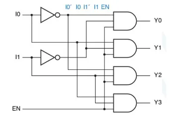
2-to-4 Decoder
Section titled “2-to-4 Decoder”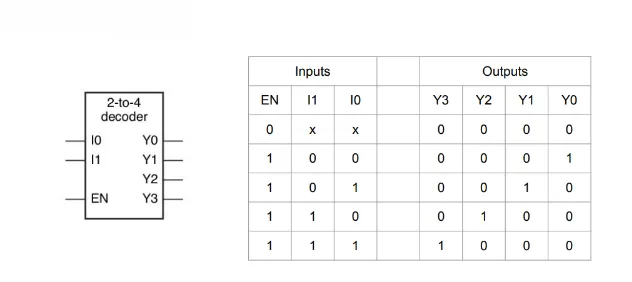
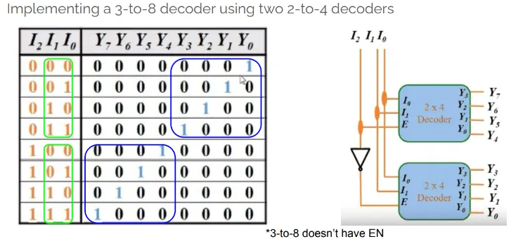
3-to-8 Decoder
Section titled “3-to-8 Decoder”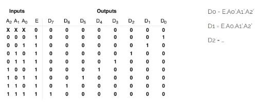
Decoder expansion
Section titled “Decoder expansion”- Each minterm → one AND gate
- Large decoders → need many-input ANDs (not practical)
- Use small decoders → build big decoder (hierarchical)
- Final AND gates → only 2 inputs
- ANDs implement minterms
Example:-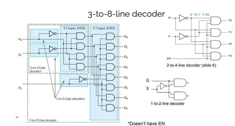
Implementing logic functions using a decoder
Section titled “Implementing logic functions using a decoder”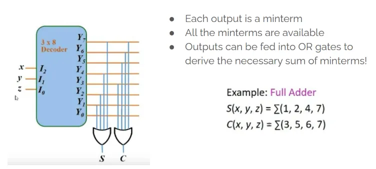
2. Encoder
Section titled “2. Encoder”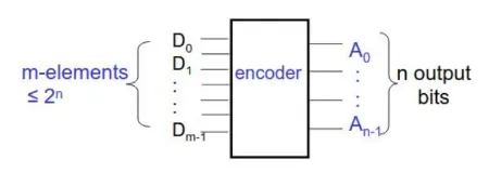 Opposite of Decoding:
- m-bit input → n-bit output (n ≤ m ≤ 2ⁿ)
- Input: one-hot (only one 1)
4-to-2 encoder
Section titled “4-to-2 encoder”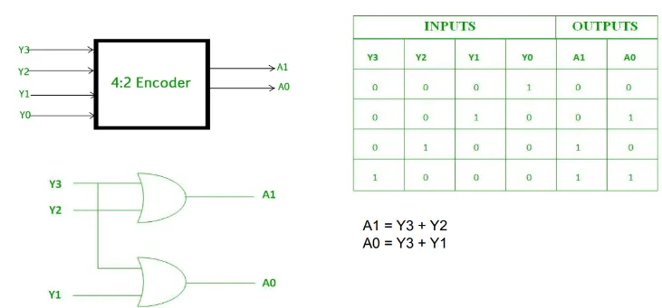
8-to-3 line encoder (octal-to-binary encoder)
Section titled “8-to-3 line encoder (octal-to-binary encoder)”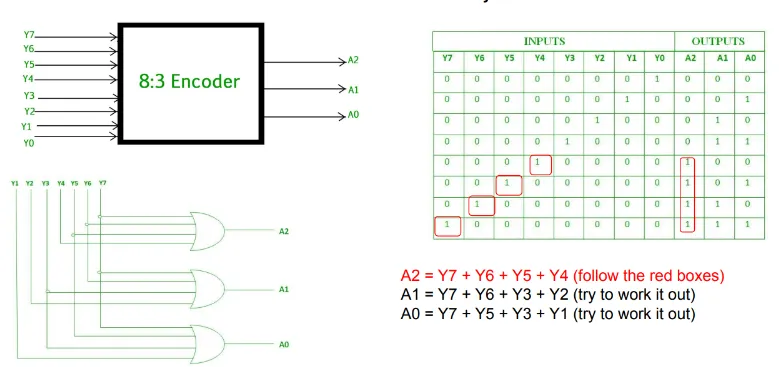
Decimal to BCD encoder
Section titled “Decimal to BCD encoder”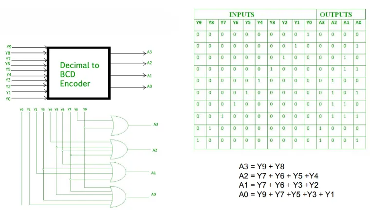
Priority encoder
Section titled “Priority encoder”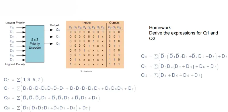
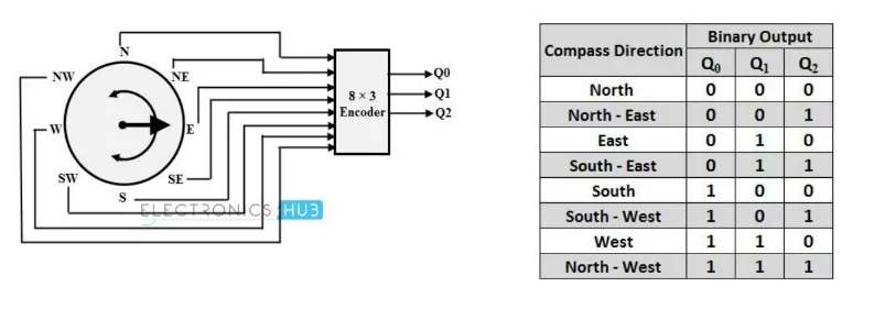
Example application:
Section titled “Example application:”- Positional encoder
3. Multiplexer (MUX)
Section titled “3. Multiplexer (MUX)”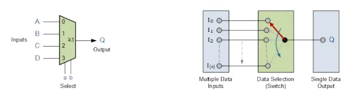
- Selects one of many input lines and forwards it to a single output.
- Controlled using select lines.
2 input MUX
Section titled “2 input MUX”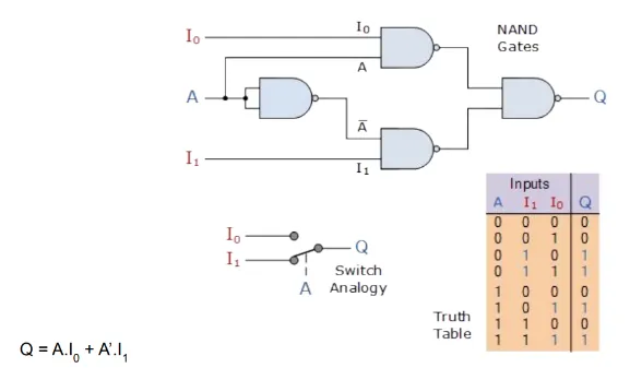
4-to-1 MUX
Section titled “4-to-1 MUX”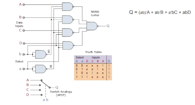
Difference between Multiplexer, Decoder, and Encoder
Section titled “Difference between Multiplexer, Decoder, and Encoder”| Feature | Multiplexer (MUX) | Decoder | Encoder |
|---|---|---|---|
| Purpose | Selects one input to pass to output | Converts binary input to 1-hot output | Converts 1-hot input to binary output |
| Inputs | Multiple data inputs, select lines | n input lines | 2ⁿ input lines |
| Outputs | Single output | 2ⁿ output lines | n output lines |
| Control Signals | Select lines | Input acts as select | No select; active input only |
| Direction | Many → 1 | n → 2ⁿ | 2ⁿ → n |
| Example Use | Data routing | Address decoding | Priority coding |
4. Digital Buffers
Section titled “4. Digital Buffers”Single input digital buffer
Section titled “Single input digital buffer”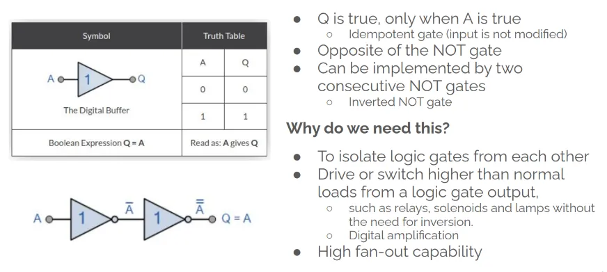
Three state (Tri State buffer)
Section titled “Three state (Tri State buffer)”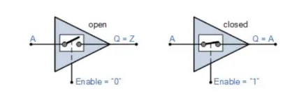
Tri-state Buffer:
- 2 logic levels (0,1), 3 output levels (0,1, High-Z)
- EN=0 → High-Z (acts like open circuit)
- Used to isolate output from bus
- Allows multiple devices to share same bus
- Common in data buses (e.g., computer peripherals)
Tri-state Digital Buffer Data Bus Control
Section titled “Tri-state Digital Buffer Data Bus Control”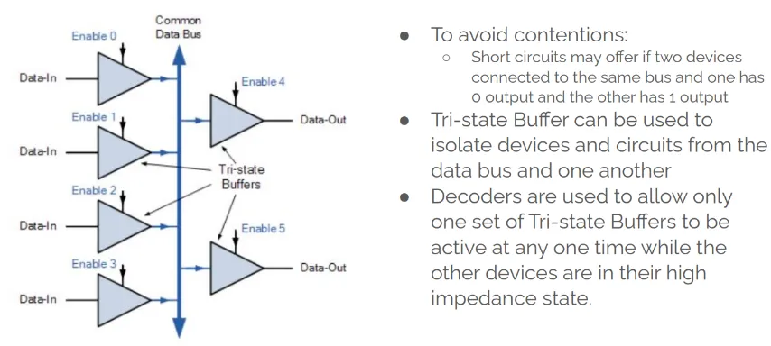
Tri-state Digital Buffer Control
Section titled “Tri-state Digital Buffer Control”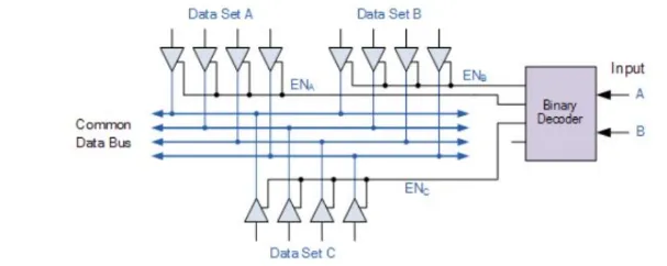
- allowing only one set of data to pass either a logic “1” or logic “0” output state onto the bus
- all the other tri-state outputs connected to the same bus lines are disabled by being placed in their high impedance Hi-Z state.
There are four types of tri-state buffers:
-
- Active High tri-state buffer
-
- Active high inverting tri-state buffer
-
- Active Low tri-state buffer
-
- Active low inverting tri-state buffer
Tri-state buffer - active high variants
Section titled “Tri-state buffer - active high variants”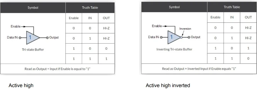
Tri-state buffer - active low variants
Section titled “Tri-state buffer - active low variants”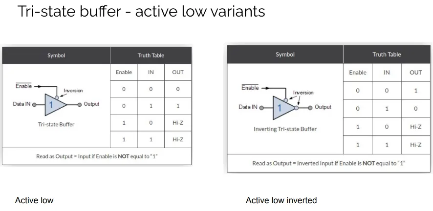
5. Comparator
Section titled “5. Comparator”- Compares two binary numbers.

Types of Comparators
Section titled “Types of Comparators”-
Equality Comparator
- Single output
- Output HIGH if A = B, else LOW
-
Magnitude Comparator
- Three outputs:
- A < B
- A = B
- A > B
- Three outputs:
1-bit magnitude comparator
Section titled “1-bit magnitude comparator”
2-bit magnitude comparator
Section titled “2-bit magnitude comparator”-
Designing
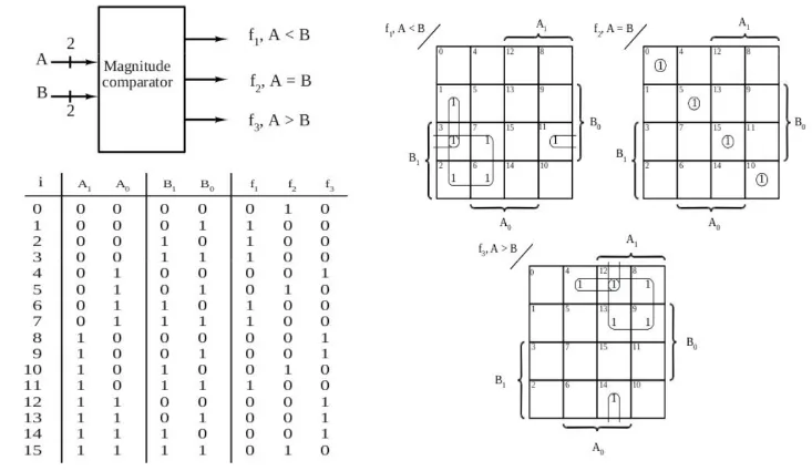
-
Realizing
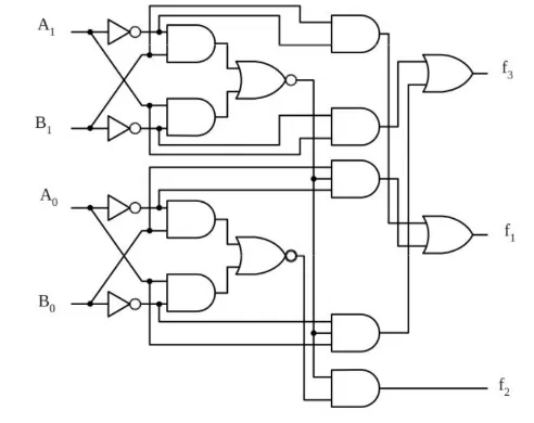
N-bit magnitude comparator
Section titled “N-bit magnitude comparator”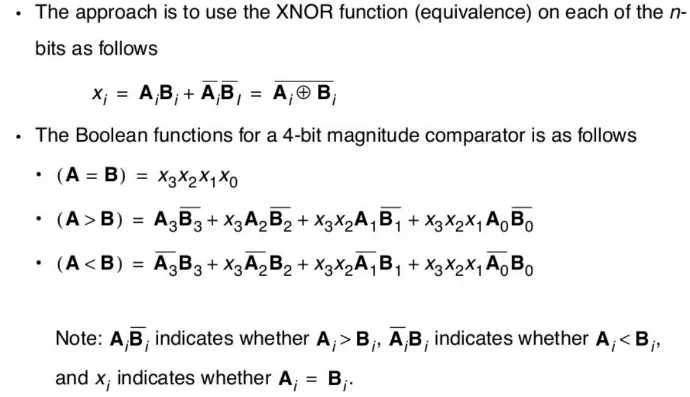
6. Adders, Subtractors, and ALUs
Section titled “6. Adders, Subtractors, and ALUs”Adders:
Section titled “Adders:”- Do binary addition
- Inputs: two or more binary numbers
- Outputs: SUM and CARRY (Cout)
Half Adder: Adds two bits.
Section titled “Half Adder: Adds two bits.”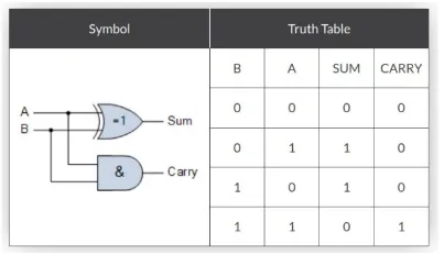
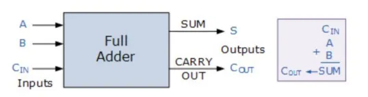
Full Adder: Adds three bits (including carry-in).
Section titled “Full Adder: Adds three bits (including carry-in).”- Has an additional input bit C in to represent a carry-in bit coming from a
previous addition step
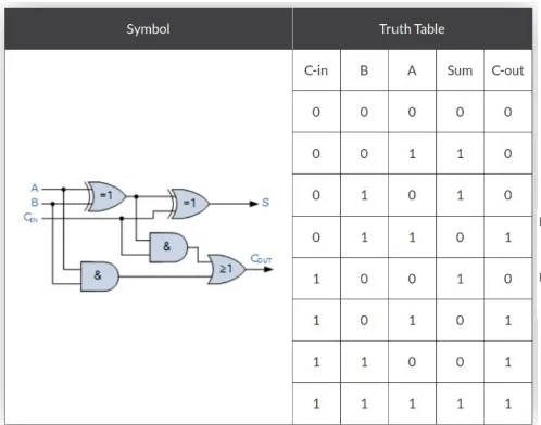
Full adder implementation with half adders
Section titled “Full adder implementation with half adders”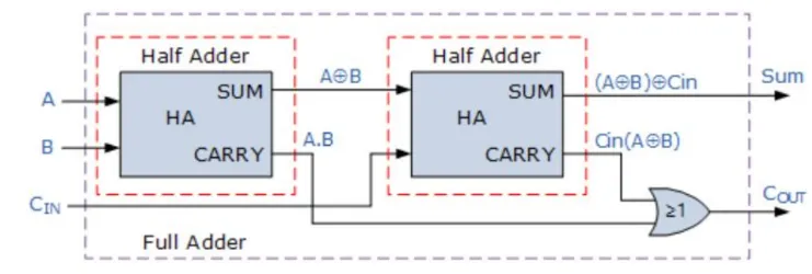
Ripple Carry Adder
Section titled “Ripple Carry Adder”- Uses n full adders connected in series
- Carry ripples from LSB to MSB (right to left)
4-bit ripple carry adder
Section titled “4-bit ripple carry adder”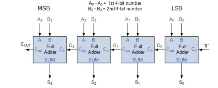
- Disadvantage: output will not be valid until any carry-input has “rippled” through every full adder in the chain
Carry Lookahead Adder (CLA)
Section titled “Carry Lookahead Adder (CLA)”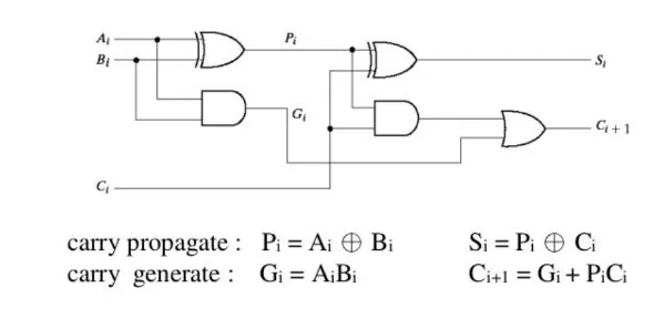
- Speeds up addition by computing carries in parallel
- No need to wait for ripple from LSB to MSB
- At each bit:
- Generate carry (from xi and yi)
- Propagate carry (pass carry-in to carry-out)
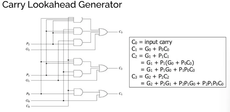
- 3 levels of delay:
- Generate & propagate signals
- Carry lookahead (sum-of-products)
- Faster than ripple carry due to parallel carry logic
Subtractors:
Section titled “Subtractors:”- A – B = A + 2’s complement of B
- 2’s complement: B’ + 1
- Circuit: Adder + inverters on B inputs
- Set input carry C0 = 1
4-bit Adder-Subtractor
Section titled “4-bit Adder-Subtractor”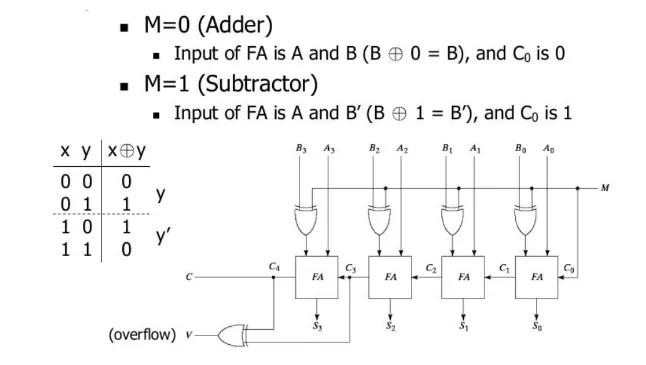
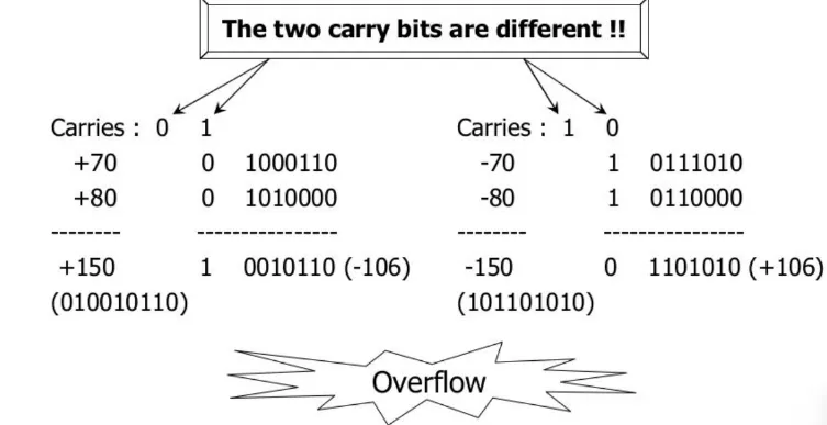
Overflow:
Section titled “Overflow:”- Happens when result > range of bits
- Common in signed binary addition/subtraction
- Detected when:
- Two positives → negative result
- Two negatives → positive result
- Example
ALUs (Arithmetic Logic Units):
Section titled “ALUs (Arithmetic Logic Units):”- Perform arithmetic and logical operations.
- Core component of a CPU.
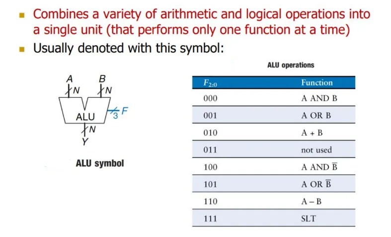
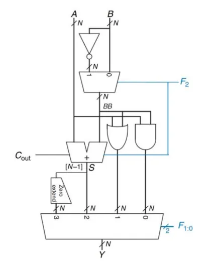
- Basic ALU Architecture
7. Lookup Tables (LUTs)
Section titled “7. Lookup Tables (LUTs)”- Memory-based way to implement logic
- Store outputs for all input combinations
- Inputs = address, output = stored value
- No need for logic gates
- Can be cascaded for complex functions
Half adder using LUTs
Section titled “Half adder using LUTs”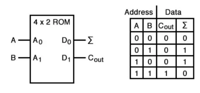
Multiplexers as LUTs
Section titled “Multiplexers as LUTs”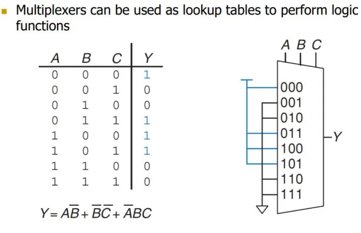
Uses of LUTs:
Section titled “Uses of LUTs:”- PLDs: Used in FPGAs/CPLDs to build custom logic
- Speed: Precomputed outputs → faster than gate-based logic
- Simplifies complex functions → fewer gates
- Function approximation → for math/nonlinear functions